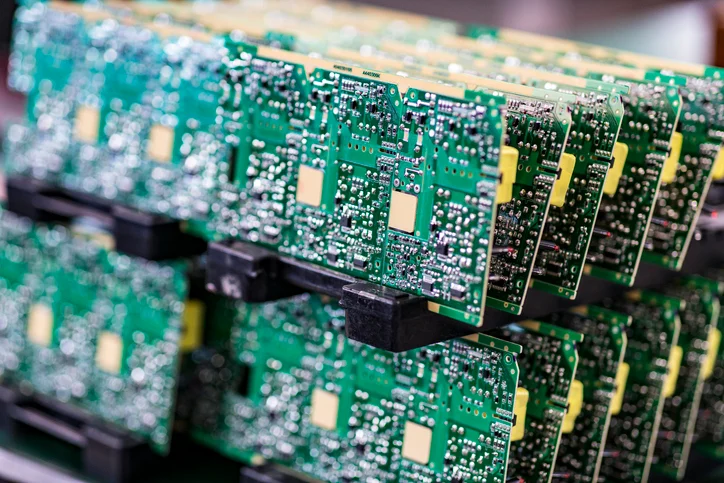
The design is, of course, the first step in any PCB manufacturing process. PCB manufacturing and design always begin with a plan: The designer prepares a layout for the printed circuit board (PCB) that meets all of the criteria that are outlined in the specifications. The form of design software known as Extended Gerber, which is also known as IX274X in certain circles, is the kind of software that is used the most commonly by PCB designers.
Extended Gerber is an excellent piece of software that can be used for PCB design. This is because, in addition to its usage as a file format, it can also be utilized in this capacity. Extended Gerber encoding stores all of the data that is required by the designer, such as the number of copper layers, solder masks, and extra component nomenclature. A few examples of this include the following: After the Gerber Extended program has encoded a view to designing for the PCB, all of the numerous aspects and features of the design are evaluated to verify that there are no faults in the overall layout.
Checking the design for potential errors or flaws is another important step in the PCB fabrication process. A technician inspects each component and structure of the PCB design to ensure there are no lacking components or incorrect structures. The design begins to move to the printing phase after receiving approval from an engineer.
The PCB design can be printed once all of the checks have been completed. PCB plans, unlike architectural drawings, do not print on a standard 8.5 x 11 sheet of paper. A plotter printer, rather than a standard printer, is used. The PCB is “filmed” by a plotter printer. The finished “film” resembles the transparencies that were once used in schools — it’s essentially a photo negative of the board itself.
After preparing the board, it is washed with an alkaline solution to remove any residual photoresists. The board is then pressure-washed to remove any remaining debris from the exterior and allowed to dry. After drying, the only resist that should persist on the PCB is on top of the copper that remains when the PCB is finally popped free.
Larger PCBs and those with thicker constructions may use more copper, resulting in more copper that must be removed via etching. As a result, these boards will necessitate additional time or solvent.
The plating process employs a chemical to bond all of the PCB’s layers together. After being thoroughly cleaned, the PCB is immersed in a series of chemicals. A micron-thick layer of copper is deposited over the topmost layer and into the holes that have just been drilled as part of the bathing process.
ChinaPCBOne handles low to medium-volume production runs from assembly to final shipment. ChinaPCBOne oversees the entire process. They complete the process, which includes design, ordering components, manufacturing, assembly, and testing.


